Indium phosphide (InP) is a remarkable semiconductor material that plays a crucial role in various advanced technologies. To understand its working principle, we need to delve into the world of semiconductors.

At the heart of InP’s functionality is its band structure. Semiconductors have a valence band and a conduction band separated by an energy gap. In the case of InP, this energy gap is relatively narrow.
When InP is in its pure state, it is an insulator. However, by introducing impurities or dopants, its electrical properties can be altered. For example, doping with donor atoms can create extra electrons in the conduction band, while doping with acceptor atoms can create holes in the valence band.
The movement of these charge carriers – electrons and holes – is what enables InP to conduct electricity. When a voltage is applied across an InP semiconductor, electrons in the conduction band and holes in the valence band are set in motion.
Electrons move towards the positive terminal, while holes move towards the negative terminal. This flow of charge carriers constitutes an electric current.
InP is particularly useful in high-frequency applications because of its high electron mobility. This means that electrons can move quickly through the material, allowing for fast signal processing and transmission.

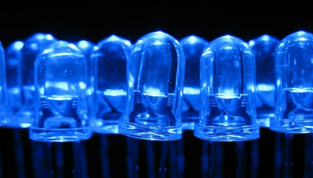
In addition to its electrical properties, InP also has excellent optical properties. It can be used to fabricate optoelectronic devices such as lasers and photodetectors. In these devices, InP’s ability to emit and detect light is exploited.
For instance, in an InP laser, electrons are excited to a higher energy state. When they return to a lower energy state, they emit photons of light. This emitted light can be used for various applications, such as optical communication.
In summary, the working principle of InP semiconductor involves the manipulation of its band structure through doping and the movement of charge carriers. Its unique properties make it an essential material for a wide range of applications in electronics and optoelectronics.


