Short Description:
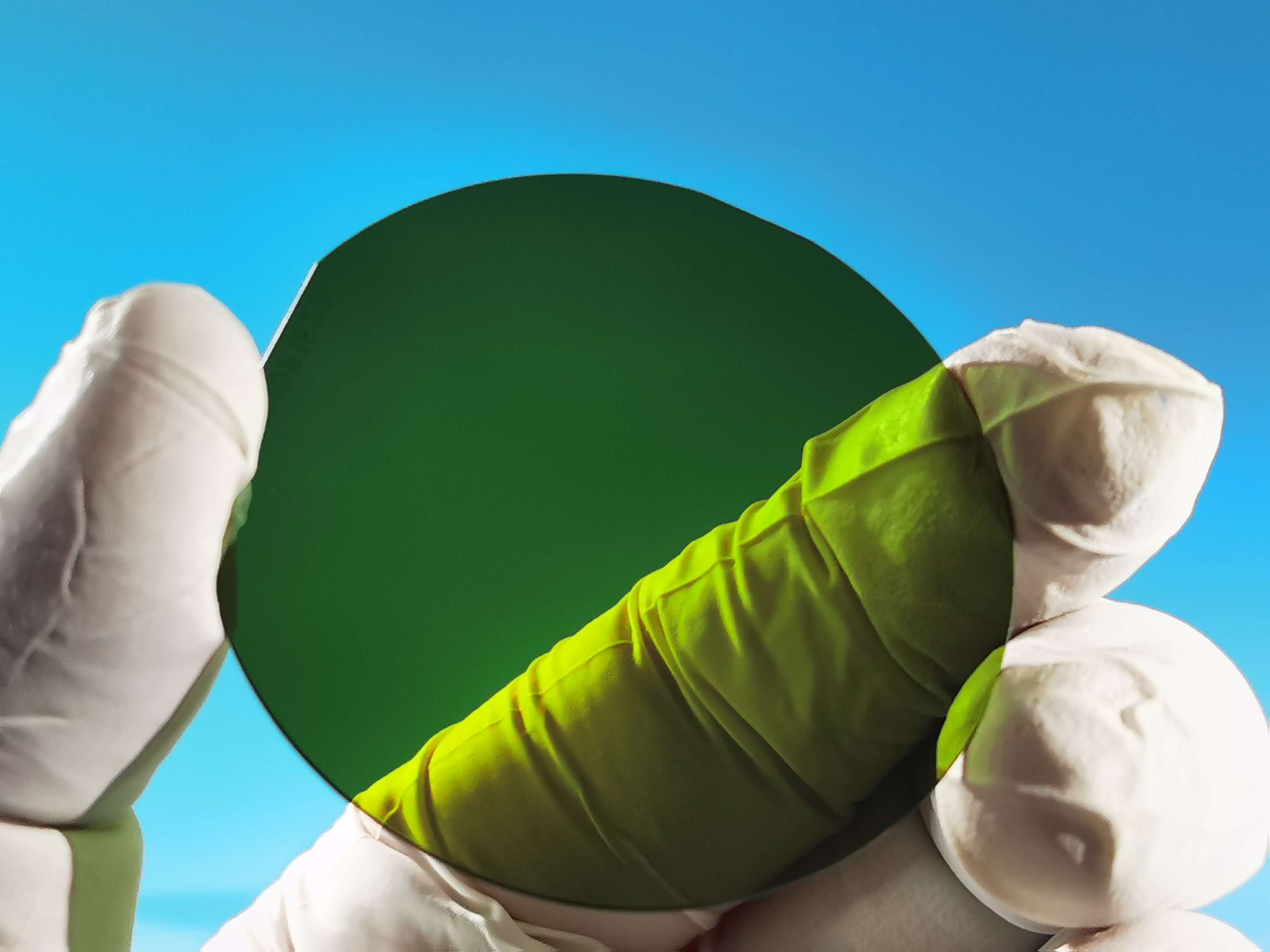
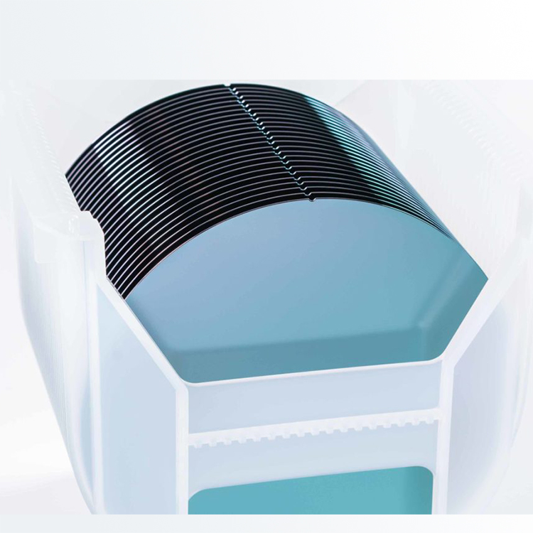
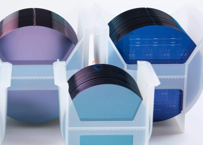
Glass substrates have a smoother surface than plastic substrates, and the number of vias is much greater in the same area than in organic materials. It is said that the spacing between through-holes in glass cores can be less than 100 microns, which directly increases the interconnect density between wafers by a factor of 10. The increased interconnect density can accommodate a greater number of transistors, allowing for more complex designs and more efficient use of space.

Glass substrates perform better in terms of thermal properties, physical stability, and are more heat resistant and less prone to warping or deformation problems due to high temperatures;
In addition, the unique electrical properties of the glass core allow for lower dielectric losses, permitting clearer signal and power transmission. As a result, power loss during signal transmission is reduced and the overall efficiency of the chip is naturally boosted. The thickness of the glass core substrate can be reduced by about half compared to ABF plastic, and the thinning improves signal transmission speed and power efficiency.
Hole forming technology of TGV:
Laser induced etching method is used to induce continuous denaturation zone through pulsed laser, and then the laser treated glass is put into hydrofluoric acid solution for etching. The etching rate of denaturation zone glass in hydrofluoric acid is faster than that of undenaturated glass to form through holes.
TGV fill:
First, TGV blind holes are made. Secondly, the seed layer was deposited inside the TGV blind hole by physical vapor deposition (PVD). Thirdly, bottom-up electroplating achieves seamless filling of TGV; Finally, through temporary bonding, back grinding, chemical mechanical polishing (CMP) copper exposure, unbonding, forming a TGV metal-filled transfer plate.
Detailed Diagram


