

In the world of semiconductor materials, silicon carbide wafers and silicon wafers play crucial roles. However, they have distinct characteristics that set them apart.

Silicon wafers have been the traditional workhorse of the semiconductor industry for many years. They are widely used due to their relatively mature technology and cost-effectiveness. Silicon is abundant in nature, making it readily available and affordable. These wafers have a well-established manufacturing process, which allows for high-volume production. Silicon wafers are suitable for a wide range of applications, from microprocessors to memory chips.
On the other hand, silicon carbide wafers are emerging as a promising alternative. One of the key differences is their superior thermal conductivity. Silicon carbide can handle much higher temperatures without degradation, making it ideal for applications where heat dissipation is a concern. This property is particularly valuable in power electronics, where high power densities and temperatures are common.
In terms of electrical properties, silicon carbide has a much higher breakdown electric field strength compared to silicon. This means it can withstand higher voltages without breaking down, enabling the design of more efficient and compact power devices. Silicon carbide also has a wider bandgap, which offers advantages in high-frequency and high-power applications.
Another difference lies in the manufacturing challenges. Silicon carbide wafers are more difficult to produce than silicon wafers. The growth process is complex and requires specialized equipment and expertise. As a result, silicon carbide wafers are currently more expensive.
In conclusion, while silicon wafers remain the dominant choice for many applications due to their maturity and cost advantages, silicon carbide wafers are gaining ground in areas where high temperature tolerance, high voltage handling, and high-frequency operation are required. As technology continues to advance, we can expect to see further developments in both types of wafers, each catering to different needs of the semiconductor industry.
碳化硅晶圆和硅晶圆的应用领域有哪些不同?
硅晶圆和碳化硅晶圆的价格比较
如何选择适合自己应用的晶圆?
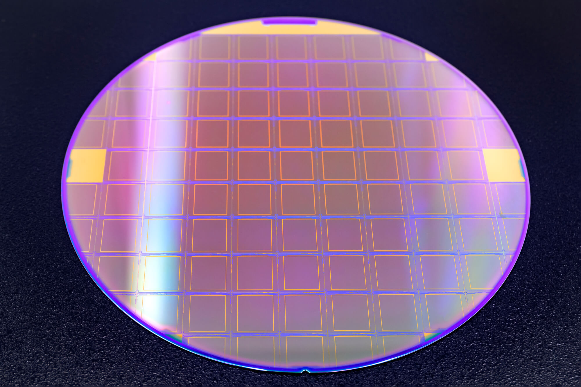


 on Silicon (Si) Epitaxy Wafer 3")
