

SiC bulk wafer ‘s description
Silicon Carbide (SiC) wafers are a crucial type of semiconductor material extensively utilized in the manufacturing of electronic and optoelectronic devices that demand high-temperature endurance, high-voltage stability, and high-frequency performance. SiC stands out as a wide-bandgap semiconductor material, characterized by a wider bandgap compared to conventional semiconductors like silicon. This attribute endows SiC with a higher breakdown voltage and the ability to function at elevated temperatures, making it ideal for rigorous applications.
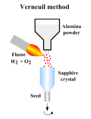
The production of SiC bulk wafer primarily employs two methods: Physical Vapor Transport (PVT) and Chemical Vapor Deposition (CVD). In the PVT method, the process begins with placing a seed crystal of SiC inside a high-temperature furnace. A source material, typically composed of silicon or carbon, is then heated until it vaporizes. This vapor is carried by a carrier gas, usually argon, and subsequently deposited on the seed crystal. This process results in the formation of a single crystal SiC layer. Conversely, the CVD method involves depositing a SiC layer on a substrate through the reaction of a gas mixture containing silicon and carbon precursors at elevated temperatures.
After the SiC crystal is successfully grown, it undergoes a series of meticulous steps to be sliced into thin wafers. These wafers are then polished to achieve a high degree of flatness and smoothness, essential for further semiconductor layer growth. The polished SiC bulk waferserve as a robust platform for the deposition of additional semiconductor layers. These layers can be precisely doped with impurities to create p-type and n-type regions, which are fundamental for the fabrication of various semiconductor devices.
SiC bulk wafers offer several significant advantages over traditional semiconductor materials such as silicon. One of the most notable benefits is SiC’s higher thermal conductivity, which allows it to sustain operation at higher temperatures without succumbing to thermal breakdown. Additionally, SiC’s higher breakdown voltage enables devices made from it to operate at much higher voltages and frequencies than those made from silicon. These properties render SiC bulk wafer particularly suitable for high-power electronics and high-frequency devices, where performance and reliability under extreme conditions are paramount.
In summary, the unique properties of SiC bulk wafer, including their high thermal conductivity, superior breakdown voltage, and the ability to function at high temperatures and frequencies, make them indispensable in advanced electronic and optoelectronic applications. The advanced manufacturing techniques such as PVT and CVD play a critical role in producing high-quality SiC bulk wafers that meet the demanding requirements of modern semiconductor devices.
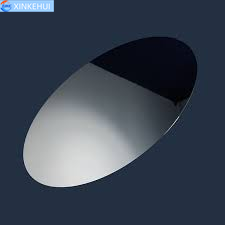
SiC bulk wafer ‘s photo


SiC bulk wafer ‘s properties
Silicon Carbide (SiC) bulk wafers possess several important properties, making them suitable for high-performance applications. Here are some key properties of SiC bulk wafers:
- Electrical Properties:
- High Bandgap: Typically around 3.0 eV, allowing operation at higher temperatures and voltages.
- High Breakdown Electric Field: Approximately 2.8-4.0 MV/cm, which enables devices to operate at higher voltages.
- High Electron Mobility: Generally between 700 and 1000 cm²/V·s, beneficial for high-frequency applications.
- Low Intrinsic Carrier Concentration: This contributes to high-temperature stability.
- Thermal Properties:
- High Thermal Conductivity: About 3-4 W/cm·K, which helps in efficient heat dissipation.
- High Melting Point: Approximately 2700°C, making it suitable for high-temperature applications.
- Mechanical Properties:
- High Hardness: SiC is one of the hardest materials, with a Mohs hardness rating of 9.0-9.5.
- High Strength and Rigidity: It has high Young’s modulus and excellent mechanical stability.
- Chemical Properties:
- High Chemical Stability: SiC is resistant to chemical attack and corrosion.
- Oxidation Resistance: It forms a protective oxide layer when exposed to oxygen at high temperatures.
- Optical Properties:
- Transparency to Infrared Radiation: Useful in certain optoelectronic applications.
- Conductivity Type:
- N-type or P-type: SiC bulk wafer can be doped to create n-type or p-type material, essential for semiconductor device fabrication.
- Crystal Structure:
- Polytypes: SiC exists in different polytypes (e.g., 4H-SiC, 6H-SiC), with 4H-SiC being the most common for electronic applications due to its superior electronic properties.
These properties make SiC bulk wafers highly suitable for applications in power electronics, high-frequency devices, high-temperature electronics, and harsh environment sensors.
| Growth Method | Physical Vapor Transport | |
| Physical Properties | ||
| Structure | Hexagonal, Single Crystal | |
| Diameter | Up to 150mm, 200mm | |
| Thickness | 350µm (n-type, 3″ SI), 500µm (SI) | |
| Grades | Prime, Development, Mechanical | |
| Thermal Properties | ||
| Thermal Conductivity | 370 (W/mK) at Room Temperature | |
| Thermal Expansion Coefficient | 4.5 (10-6K-1) | |
| Specific Heat (25⁰C) | 0.71 (J g-1 K-1) | |
| Additional Key Properties of II-VI SiC Substrates (typical values*) | ||
| Parameter | N-type | Semi-insulating |
| Polytype | 4H | 4H, 6H |
| Dopant | Nitrogen | Vanadium |
| Resistivity | ~0.02 Ohm-cm | > 1∙1011 Ohm-cm |
| Orientation | 4° off-axis | On-axis |
| FWHM | < 20 arc-sec | < 25 arc-sec |
| Roughness, Ra** | < 5 Å | < 5 Å |
| Dislocation density | ~5∙103 cm-2 | < 1∙104 cm-2 |
| Micropipe density | < 0.1 cm-2 | < 0.1 cm-2 |
SiC bulk wafer ‘s application
Silicon Carbide (SiC) bulk wafers are increasingly being utilized across a wide range of applications, particularly in areas that demand high performance under extreme conditions. Here are some key applications of SiC bulk wafers:
High-Power Electronics
- Power Devices: SiC bulk wafers are used to fabricate power devices like MOSFETs, Schottky diodes, and thyristors. These devices benefit from SiC’s high breakdown voltage and thermal conductivity, making them ideal for applications in power converters, inverters, and motor drives.
- Electric Vehicles (EVs): SiC-based power electronics in EVs improve efficiency, reduce weight, and extend the driving range. SiC MOSFETs and diodes are increasingly used in onboard chargers and powertrain inverters.
- Renewable Energy Systems: In photovoltaic inverters and wind turbine converters, SiC devices enhance efficiency and reliability, which are critical for sustainable energy applications.

High-Frequency Devices
- RF and Microwave Devices: SiC bulk wafer are used in radio frequency (RF) and microwave power amplifiers. Their high-frequency performance makes them suitable for wireless communication, radar, and satellite communication systems.
- Telecommunications: SiC technology supports high-frequency operation in 5G networks and beyond, providing improved signal processing capabilities and bandwidth.

High-Temperature and Harsh Environment Electronics
- Aerospace and Defense: SiC-based components are used in aerospace applications due to their ability to operate reliably under high temperatures and radiation environments. This includes applications in aircraft, spacecraft, and missile systems.
- Industrial Electronics: In industrial settings, SiC devices are used in motor control, power supplies, and high-temperature sensors, where robustness and reliability are essential.

Optoelectronics
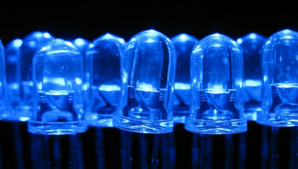
- LEDs and Solid-State Lighting: SiC substrates are used for the growth of high-brightness blue and ultraviolet LEDs. They provide a lattice match for gallium nitride (GaN) epitaxial layers, enhancing the performance and efficiency of LEDs.
- Laser Diodes: SiC bulk wafer serve as substrates for laser diodes, which are used in various applications, including medical devices, telecommunications, and data storage.

Automotive Electronics
- Power Management: SiC devices are integral in automotive power management systems, providing efficient energy conversion and power distribution.
- Battery Management Systems (BMS): In electric and hybrid vehicles, SiC-based components enhance the performance and reliability of BMS, crucial for battery health and longevity.

Renewable Energy
- Photovoltaic Systems: SiC bulk wafer devices are used in solar inverters, improving the efficiency of converting DC electricity generated by solar panels into AC electricity used in the grid.
- Wind Energy: In wind turbine converters, SiC bulk wafer components enhance efficiency and reduce weight, contributing to more effective energy conversion.

Industrial Applications
- Induction Heating: SiC’s ability to withstand high temperatures makes it suitable for induction heating applications used in industrial processing.
- Welding Equipment: SiC-based power electronics improve the performance and reliability of welding equipment, enabling better control and energy efficiency.

Consumer Electronics
- Fast Chargers: SiC bulk wafer technology is employed in fast chargers for consumer electronics, providing higher efficiency and faster charging times.
- Power Adapters: SiC-based power adapters offer compact, efficient solutions for various consumer electronic devices.

In summary, Silicon Carbide (SiC) bulk wafers play a crucial role in enhancing the performance and efficiency of devices across a wide array of sectors. These include high-power and high-frequency electronics, optoelectronics, automotive, renewable energy, and various industrial applications. The distinct properties of SiC bulk wafer, such as its wide bandgap, high thermal conductivity, and superior breakdown voltage, make it an exceptional material for applications that require high efficiency, high temperature endurance, and high voltage operation.
Q&A
What is the difference between SI and SiC bulk wafer?
Silicon (Si) wafers and Silicon Carbide (SiC) wafers are both fundamental materials used in the semiconductor industry, but they differ significantly in their properties, applications, and the technologies they enable. Here’s an in-depth comparison of the two:
Material Properties
Silicon (Si) Wafers
- Crystal Structure: Silicon has a diamond cubic crystal structure.
- Bandgap: Silicon has a bandgap of about 1.1 eV, which is relatively narrow.
- Thermal Conductivity: Silicon has a moderate thermal conductivity of about 150 W/mK.
- Breakdown Voltage: Silicon has a lower breakdown voltage compared to SiC.
- Electrical Properties: Silicon has good electrical conductivity, which can be modified by doping with other elements.
Silicon Carbide (SiC) Wafers
- Crystal Structure: SiC has a more complex crystal structure with many polytypes, the most common being 4H-SiC and 6H-SiC.
- Bandgap: SiC has a wider bandgap of about 2.3-3.3 eV depending on the polytype, making it a wide-bandgap semiconductor.
- Thermal Conductivity: SiC bulk wafer has a high thermal conductivity of about 490 W/mK.
- Breakdown Voltage: SiC bulk wafer can handle much higher breakdown voltages, typically 10 times greater than silicon.
- Electrical Properties: SiC bulk wafer also has good electrical conductivity, which can be controlled through doping, but it is inherently higher resistivity than silicon.
Manufacturing Processes
Silicon (Si) Wafers
- Production Method: Silicon wafers are typically produced using the Czochralski (CZ) process or the Float Zone (FZ) process.
- Raw Material: The starting material is highly pure silicon, often derived from quartz or sand.
- Process Steps: Involves melting the raw silicon, pulling a single crystal ingot, slicing the ingot into wafers, and polishing the wafers.
Silicon Carbide (SiC) Wafers
- Production Method: SiC bulk wafer are produced using methods such as Physical Vapor Transport (PVT) and Chemical Vapor Deposition (CVD).
- Raw Material: The raw materials are silicon and carbon sources.
- Process Steps: SiC crystal growth involves high-temperature processes to sublimate the raw materials and deposit them on a seed crystal, followed by slicing and polishing the grown crystal.
Performance Characteristics
Silicon (Si) Wafers
- Operating Temperature: Silicon devices typically operate up to about 150°C.
- Switching Speed: Silicon devices have slower switching speeds compared to SiC.
- Thermal Management: Silicon requires more robust cooling systems due to lower thermal conductivity.
Silicon Carbide (SiC) Wafers
- Operating Temperature: SiC devices can operate at much higher temperatures, often exceeding 300°C.
- Switching Speed: SiC devices can switch faster due to their higher electron mobility.
- Thermal Management: SiC’s high thermal conductivity reduces the need for extensive cooling systems.
Applications
Silicon (Si) Wafers
- Consumer Electronics: Widely used in microprocessors, memory devices, and various integrated circuits found in smartphones, computers, and other consumer electronics.
- Photovoltaics: Silicon is the primary material used in solar cells for converting sunlight into electricity.
- Standard Power Electronics: Used in power diodes, transistors, and rectifiers in general power management applications.
Silicon Carbide (SiC) Wafers
- High-Power Electronics: Essential for high-power, high-voltage applications such as power inverters, motor drives, and uninterruptible power supplies (UPS).
- Automotive: Used in electric vehicle (EV) powertrains, chargers, and battery management systems due to their efficiency and ability to handle higher voltages.
- Aerospace and Defense: Suitable for high-temperature, high-radiation environments, making them ideal for aerospace and military applications.
- Renewable Energy: Employed in photovoltaic inverters and wind turbine converters for efficient energy conversion.
- RF and Microwave Devices: Used in telecommunications and radar systems due to their high-frequency capabilities.
Cost and Market Considerations
Silicon (Si) Wafers
- Cost: Silicon wafers are generally less expensive to produce due to well-established manufacturing processes and economies of scale.
- Market Maturity: Silicon technology is mature, with extensive infrastructure and widespread adoption in various industries.
Silicon Carbide (SiC) Wafers
- Cost: SiC bulk wafers are more expensive due to more complex manufacturing processes and lower production volumes.
- Market Growth: The market for SiC is growing rapidly, driven by the demand for high-efficiency, high-performance devices in automotive, renewable energy, and other sectors.
Challenges
Silicon (Si) Wafers
- Temperature Limitations: Silicon’s performance degrades at high temperatures.
- Voltage Limitations: Silicon devices have lower breakdown voltages, limiting their use in high-power applications.
Silicon Carbide (SiC) Wafers
- Manufacturing Complexity: Producing high-quality SiC bulk wafers is more challenging, involving higher temperatures and more complex processes.
- Defects: SiC crystals are more prone to defects, which can affect device performance and yield.
Future Prospects
Silicon (Si) Wafers
- Continued Dominance: Silicon is expected to remain dominant in many applications, especially in consumer electronics and photovoltaics, due to its cost-effectiveness and established technology base.
- Innovations: Ongoing innovations in silicon technology aim to improve efficiency and performance, such as silicon-on-insulator (SOI) and advanced doping techniques.
Silicon Carbide (SiC) Wafers
- Expanding Applications: SiC is expected to see increased adoption in high-power and high-temperature applications, driven by advancements in production technology and cost reductions.
- Technological Improvements: Continued research and development are likely to reduce defects and improve the quality and affordability of SiC bulk wafers.
In summary, while both Si and SiC bulk wafer are critical to the semiconductor industry, they serve different roles based on their unique properties. Silicon remains the go-to material for a wide range of standard applications due to its cost-effectiveness and well-established manufacturing processes. In contrast, SiC is increasingly favored for demanding applications where high efficiency, high temperature, and high voltage performance are essential. As technology advances, the use of SiC is expected to grow, complementing silicon in the ever-evolving landscape of semiconductor devices.
What are 3 types of silicon wafers?
Silicon wafers come in various types, each designed for specific applications and manufacturing processes. Here are three common types of silicon wafers:
1. Monocrystalline Silicon Wafers
Characteristics:
- Structure: Composed of a single continuous crystal lattice without grain boundaries.
- Production Method: Typically produced using the Czochralski (CZ) process or the Float Zone (FZ) process.
- Purity: High purity, essential for electronic devices.
Applications:
- Semiconductors: Used in the manufacturing of integrated circuits (ICs) and microprocessors.
- Solar Cells: High-efficiency monocrystalline solar cells.
- MEMS Devices: Micro-electromechanical systems used in sensors and actuators.
Advantages:
- Electrical Performance: Superior electrical properties due to minimal defects and impurities.
- Efficiency: Higher efficiency in solar cells and electronic devices.
Disadvantages:
- Cost: More expensive to produce than polycrystalline silicon wafers.
- Production Complexity: Requires precise and controlled manufacturing processes.
2. Polycrystalline Silicon Wafers
Characteristics:
- Structure: Consists of multiple small silicon crystals or grains.
- Production Method: Produced by melting silicon and casting it into molds, followed by slicing.
- Purity: Lower purity compared to monocrystalline silicon.
Applications:
- Solar Cells: Widely used in the production of cost-effective photovoltaic panels.
- Basic Electronics: Utilized in some less demanding electronic applications.
Advantages:
- Cost: Lower production cost compared to monocrystalline silicon wafers.
- Production Ease: Simpler manufacturing process.
Disadvantages:
- Efficiency: Lower efficiency and electrical performance due to grain boundaries.
- Defects: More susceptible to impurities and defects.
3. Silicon-on-Insulator (SOI) Wafers
Characteristics:
- Structure: Comprises a thin layer of silicon separated from the bulk silicon wafer by an insulating layer of silicon dioxide.
- Production Method: Created using techniques like Separation by IMplantation of OXygen (SIMOX) or Smart Cut™.
- Purity: High-quality silicon layer with reduced parasitic capacitance.
Applications:
- Advanced Microelectronics: Used in high-performance, low-power ICs.
- MEMS Devices: Common in the production of MEMS for better isolation and performance.
- Optoelectronics: Useful in photonic devices and integrated circuits.
Advantages:
- Performance: Enhanced speed and reduced power consumption due to minimized parasitic capacitance.
- Isolation: Improved device isolation, reducing cross-talk and noise.
Disadvantages:
- Cost: Higher cost due to complex manufacturing processes.
- Thermal Management: Potential issues with heat dissipation compared to bulk silicon.
Summary
These three types of silicon wafers—monocrystalline, polycrystalline, and silicon-on-insulator—each have distinct properties and applications. Monocrystalline wafers are prized for their high purity and efficiency in electronics and solar cells. Polycrystalline wafers offer a cost-effective solution for photovoltaic applications, albeit with lower efficiency. Silicon-on-insulator wafers provide significant advantages in advanced microelectronics and MEMS devices due to their superior electrical isolation and performance characteristics. Each type of wafer is tailored to meet specific needs within the semiconductor industry.
p-type 4H/6H-P 3C-N TYPE SIC substrate 4inch 〈111〉± 0.5°Zero MPD 8inch SiC wafer Silicon Carbide Wafer prime dummy research grade 500um 350 um Silicon carbide wafers have both C-face and Si-face orientations because of the way they are grown.