


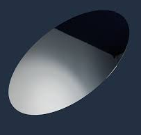
In the realm of modern technology, InP (Indium Phosphide) semiconductor stands out as a remarkable material with extraordinary properties and immense potential.

Indium Phosphide is a key player in the semiconductor industry due to its unique characteristics. It has a high electron mobility and a relatively narrow bandgap compared to some other semiconductors. This combination allows for efficient transmission of electrical signals and makes InP highly suitable for high-frequency applications.
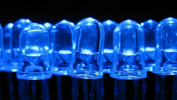
One of the significant areas where InP shines is in optoelectronics. It is widely used in the fabrication of lasers and photodetectors. InP-based lasers are capable of emitting light at specific wavelengths, making them essential for optical communication systems. These lasers offer high-speed data transmission and long-distance signal propagation, enabling the seamless flow of information in today’s digital age.
Moreover, InP photodetectors are highly sensitive and can detect even weak optical signals. They find applications in a variety of fields, including telecommunications, astronomy, and medical imaging. The ability of InP to efficiently convert light into electrical signals makes it an invaluable component in these applications.
In addition to optoelectronics, InP also plays a crucial role in high-speed electronics. Its high electron mobility enables faster switching speeds and lower power consumption, making it ideal for use in advanced microprocessors and high-frequency amplifiers. As the demand for faster and more efficient electronic devices continues to grow, InP is likely to become even more important in the future.
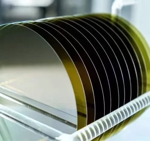
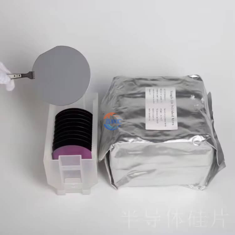
The production of InP semiconductors requires advanced manufacturing techniques. The material is typically grown using methods such as metalorganic vapor phase epitaxy (MOVPE) or molecular beam epitaxy (MBE). These processes allow for precise control over the crystal structure and properties of InP, ensuring high-quality materials for various applications.
Despite its many advantages, InP also faces some challenges. The cost of production can be relatively high compared to other semiconductors, and the material can be difficult to process. However, ongoing research and development efforts are focused on addressing these issues and making InP more accessible and cost-effective.
In conclusion, InP semiconductor is a remarkable material that holds great promise for the future of technology. Its unique properties make it essential in optoelectronics and high-speed electronics, and ongoing research is likely to unlock even more applications. As we continue to push the boundaries of technology, InP will undoubtedly play a crucial role in shaping the future of the semiconductor industry.

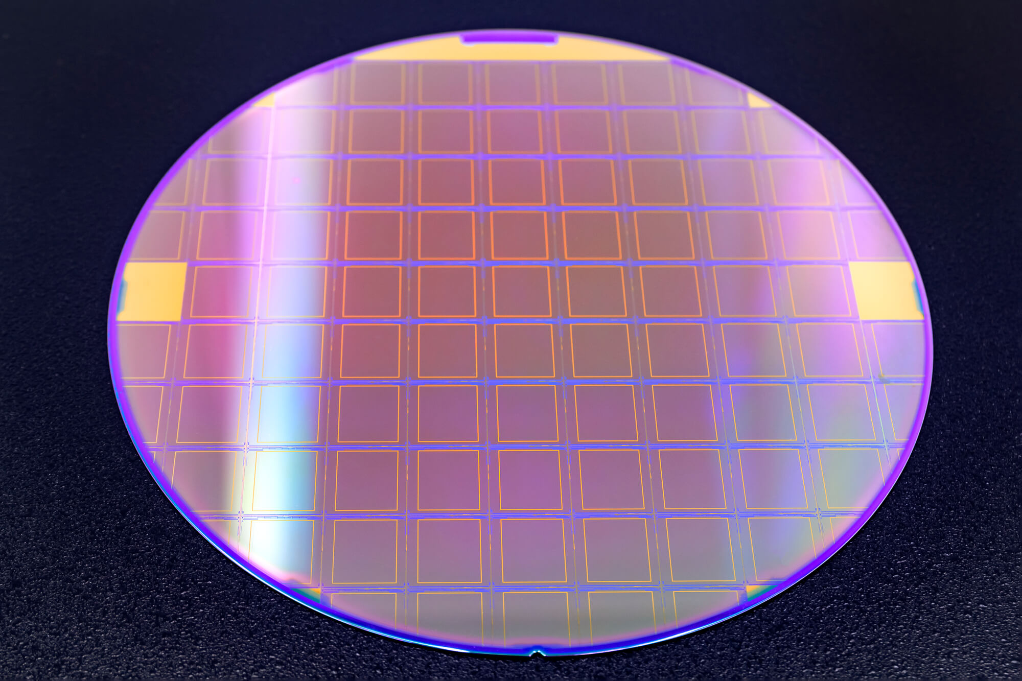


 on Silicon (Si) Epitaxy Wafer 4")
