

Etching silicon wafer‘s abstarct

XINKEHUI’s etching silicon wafers are meticulously designed to meet high industry standards, available in both N type and P type classifications. These wafers are engineered to have an exceptionally low surface roughness, which enhances their utility in sensitive electronic applications. The wafers are offered with options for both low and high reflectivity, allowing them to be optimally used in various technological environments depending on the specific light absorption and reflection needs.
The standout feature of these etching wafers is their remarkable glossiness coupled with a relatively low production cost. This combination makes them highly desirable as they provide a cost-effective alternative to more expensive polished or epitaxial wafers. By substituting these higher-cost wafers, XINKEHUI’s etching wafers offer a significant cost advantage in manufacturing processes, particularly in the production of electronic elements where reducing expenses without sacrificing quality is crucial.
Furthermore, the adoption of these etching wafers can lead to substantial cost savings in the mass production of electronic components, especially in industries looking to optimize material costs while maintaining high performance and reliability in their electronic devices. This makes XINKEHUI’s etching silicon wafers an invaluable resource for companies aiming to enhance their competitive edge in the market.
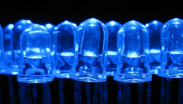
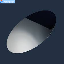
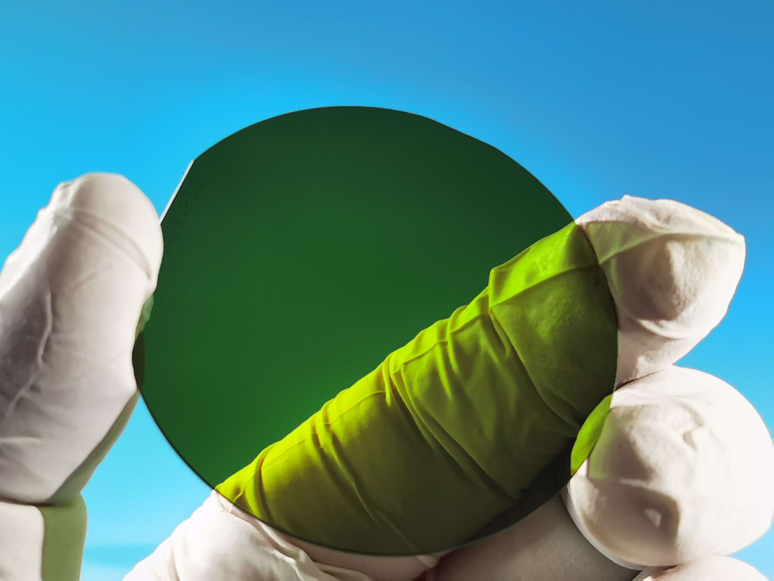
Etching Silicon Wafers’ photos


Etching silicon wafer‘s properties
- Material Composition: Typically made from high-purity Etching Silicon Wafers, which is essential for achieving the desired electrical properties in semiconductor devices.
- Surface Smoothness: Etching wafers often have extremely smooth surfaces, which is crucial for the deposition of thin films and other materials in device fabrication.
- Dimensional Stability: They maintain their shape and dimensions under the thermal and chemical stresses encountered during various manufacturing processes.
- Thermal Conductivity: Etching Silicon Wafers has good thermal conductivity, which helps dissipate heat generated during device operation, thereby enhancing performance and longevity.
- Electrical Properties: The intrinsic semiconductor nature of Etching Silicon Wafers can be modified through doping to create either p-type or n-type materials, which are fundamental for forming p-n junctions in electronic devices.
- Chemical Resistance: Etching Silicon Wafers is resistant to oxidation and other chemical reactions at room temperature, although it can be etched with specific chemicals under controlled conditions, which is how patterns are created on the wafer.
- Mechanical Strength: Despite being relatively brittle, Etching Silicon Wafers are strong enough to withstand handling and processing without degrading their usability.
Silicon (Si) is the predominant semiconductor material used in the technology industry, notable for its ability to be processed into single crystal wafers up to 450 mm in diameter. These wafers are remarkably thin, typically less than 1 mm in thickness, and are circular slices derived from a larger single crystal semiconductor ingot. The geometric arrangement of silicon atoms within the crystal is organized into lattice planes and directions, which are mathematically represented using the Miller Index. This indexing system provides a way to describe vectors normal to the surfaces of specific crystal planes or facets within the cubic lattice structure of the Etching Silicon Wafers.
In this cubic system, a notation such as [hkl] is employed to denote the orientation of a plane or facet, simplifying the characterization and manipulation of the crystal for various applications. Each silicon crystal is composed of fundamental units that repeat periodically, each with a distinct shape, volume, and composition. These fundamental units are crucial for understanding and exploiting the electronic properties of Etching Silicon Wafersin semiconductor manufacturing. This structured approach to describing and cutting the wafers ensures precision in the creation of semiconductor devices, where consistency and accuracy are paramount.
Crystal Properties
| Property | Value | Units |
|---|---|---|
| Structure | Cubic | |
| Space Group | Fd3m | |
| Atomic weight | 28.0855 | |
| Lattice spacing (a0) at 300K | 0.54311 | nm |
| Density at 300K | 2.3290 | g/cm3 |
| Nearest Neighbour Distance at 300K | 0.235 | nm |
| Number of atoms in 1 cm3 | 4.995×10²² | |
| Isotopes | 28 (92.23%) 29 (4.67%) 30 (3.10%) |
|
| Electron Shells | 1s22s22p63s23p2 | |
| Common Ions | Si 4 +, Si 4 – | |
| Critical Pressure | 1450 | atm |
| Critical Temperature | 4920 | °C |
Band Structure Properties
| Property | Value | Units |
|---|---|---|
| Dielectric Constant at 300 K (Relative Permittivity (εr)) | 11.7 | |
| Dielectric Strength | 100 – 700 | (V/mil) |
| Loss Tangent | 0.005 (at 1 GHz) 0.015 (at 10 GHz) |
|
| Effective density of states (conduction, Nc T=300 K ) | 2.8×10¹⁹ | cm-3 |
| Effective density of states (valence, Nv T=300 K ) | 1.04×10¹⁹ | cm-3 |
| Electron affinity | 133.6 | kJ / mol |
| Energy Gap Eg at 300 K (Minimum Indirect Energy Gap at 300 K) | 1.12 | eV |
| Energy Gap Eg at ca. 0 K (Minimum Indirect Energy Gap at 0K) | 1.17 (at 0 K) | eV |
| Minimum Direct Energy Gap at 300 K | 3.4 | eV |
| Energy separation (EΓL) | 4.2 | eV |
| Intrinsic Debye length | 24 | µm |
| Intrinsic carrier concentration at 300K | 1×10¹⁰ | cm-3 |
| Intrinsic carrier concentration at 25°C | 8.6×10⁹ | cm-3 |
| Intrinsic resistivity | 3.2×10⁵ | Ω×cm |
| Auger recombination coefficient Cn | 1.1×10⁻³⁰ | cm6 / s |
| Auger recombination coefficient Cp | 3×10-31 | cm6 / s |
Thermal Properties
| Property | Value | Units |
|---|---|---|
| Melting point | 1414 1687 |
°C K |
| Boiling point | 3538 | K |
| Specific heat | 0.7 | J / (g × °C) |
| Thermal conductivity [300K] | 148 | W / (m × K) |
| Thermal diffusivity | 0.8 | cm2/s |
| Thermal expansion, linear | 2.6×10⁻⁶ | °C -1 |
| Debye temperature | 640 | K |
| Temperature dependence of band gap | -2.3e-4 | eV/K |
| Heat of: fusion / vaporization / atomization | 39.6 / 383.3 / 452 | kJ / mol |
Electrical Properties
| Property | Value | Units |
|---|---|---|
| Breakdown field | ≈ 3×10⁵ | V/cm |
| Index of refraction | 3.42 | |
| Mobility electrons | ≈ 1400 | cm2 / (V × s) |
| Mobility holes | ≈ 450 | cm2 / (V × s) |
| Diffusion coefficient electrons | ≈ 36 | cm2/s |
| Diffusion coefficient holes | ≈ 12 | cm2/s |
| Electron thermal velocity | 2.3×10⁵ | m/s |
| Electronegativity | 1.8 | Pauling`s |
| Hole thermal velocity | 1.65×10⁵ | m/s |
| Optical phonon energy | 0.063 | eV |
| Density of surface atoms | (100) 6.78 (110) 9.59 (111) 7.83 |
1014/cm2 1014/cm2 1014/cm2 |
| Work function (intrinsic) | 4.15 | eV |
| Ionization Energies for Various Dopants | Donors:Sb 0.039 P 0.045 As 0.054 Acceptors:B 0.045 Al 0.067 Ga 0.072 In 0.16 |
eV eV eV eV |
Mechanical Properties
| Property | Value | Units | |
|---|---|---|---|
| Bulk modulus of elasticity | 9.8×10¹¹ | dyn/cm2 | |
| Density | 2.329 | g/cm3 | |
| Hardness | 7 | on the Mohs scale | |
| Surface microhardness (using Knoop’s pyramid test) | 1150 | kg/mm2 | |
| Elastic constants | C11 = 16.60×10¹¹ C12 = 6.40×10¹¹ C44 = 7.96×10¹¹ |
dyn/cm2 dyn/cm2 dyn/cm2 |
|
| Young’s Modulus (E) | [100] [110] [111] |
129.5 168.0 186.5 |
GPa GPa GPa |
| Shear Modulus | 64.1 | GPa | |
| Poisson’s Ratio | 0.22 to 0.28 | ||
Our Etching Silicon Wafers manufacturing process
From sand to ingot
Silicon, constituting about 27% of the Earth’s crust, ranks as the second most abundant element, following oxygen. It does not occur in its elemental form naturally but exists predominantly as silicon dioxide (SiO2). This compound forms a significant part of sand and various types of rocks.
For its application in the semiconductor industry, silicon must be extracted and refined to achieve an ultra-high purity level of approximately 99.9999999% (9N). This purification process involves three energy-intensive steps:
- step1 Sand to Metallurgical grade Silicon
Silica sand, which naturally contains at least 98% SiO2, is mined in locations that are strategically chosen for their ease of transportation by ship, such as Mexico. The sand is then transported to regions where hydroelectric power is abundant and cost-effective, like the west coast of Norway. Here, the sand is introduced into electric arc furnaces equipped with large carbon electrodes. At high temperatures, a chemical reaction occurs where SiO2 and carbon combine to produce silicon and carbon monoxide, as described by the equation SiO2 + 2C → Si + 2CO. The silicon produced through this process is of metallurgical grade, which is about 99% pure, and is primarily used in the hardening processes of aluminum and steel.
- step 2 Metalurgical to Semiconductor grade Silicon (Siemens process)
Metallurgical grade silicon is subjected to a reaction with hydrogen chloride, typically resulting in the formation of trichlorosilane (TCS), as shown by the chemical equation Si + 3HCl → SiHCl3 + H2. TCS, which is a liquid, undergoes several stages of distillation, increasing in purity from the initial 2N (99%) to an impressive 9N (99.9999999%) purity.
This ultra-pure TCS vapor is then directed over heated silicon rods at a temperature of 1,150ºC. At this high temperature, the TCS dissociates, and silicon begins to deposit on the rods as small crystals. The volatile by-products of this reaction are captured, redistilled, and recycled to enhance efficiency and reduce waste.
As the silicon rods accumulate more silicon, they grow in size to diameters of either 100mm or 200mm. Once they reach the desired size, they are either used directly for the Float-Zone (FZ) crystallization method or crushed into smaller pieces for use in the Czochralski (CZ) crystallization process. This method of producing high-purity silicon is known as the Siemens process, which is the most common technique for manufacturing semiconductor-grade silicon.
- step3 Monocrystalline Silicon ingots
Polycrystalline silicon is transformed into monocrystalline ingots primarily using the Czochralski (CZ) process. In this method, chunks of polysilicon along with a selected dopant are placed into a quartz crucible and melted in an electric furnace under an argon atmosphere. A seed crystal is then carefully inserted into the molten silicon, slowly rotated, and gradually lifted. As it is withdrawn, silicon crystallizes around it, forming a cylindrical single-crystal ingot. The diameter of these ingots can be up to 300mm or even 450mm, depending on the process settings.
The crystallographic orientation of the ingot matches that of the seed crystal, which can be oriented in the (100), (111), (110), or (211) planes. A precise and controlled amount of a dopant—such as Boron, Phosphorus, Antimony, or Arsenic—is added to the silicon to tailor its electrical conductivity to specific requirements.
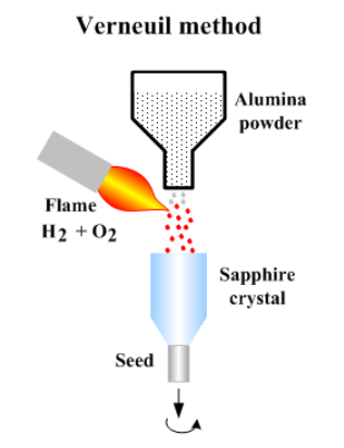
The Floating Zone (FZ) technique is another method used for growing high-purity monocrystalline silicon ingots, especially when high resistivity or minimal oxygen contamination is needed. This crucible-free method involves maintaining a molten zone of silicon between two solid rods, using only surface tension. Dopants are introduced into this zone through a gas, enhancing the ingot’s properties without the risk of oxygen contamination from a quartz crucible, a common issue with the CZ process.
From ingot to wafer
Silicon ingots are produced in a variety of sizes, with common nominal diameters including 1″, 2″, 3″, 100mm, 125mm, 150mm, 200mm, 300mm, and 450mm. These ingots are typically crystallized using either the Czochralski (CZ) or Floating Zone (FZ) methods. The crystallographic orientations of the ingots are primarily (100) or (111), though (110) and (211) orientations are also used.
To achieve p-type conductivity, silicon ingots are doped with Boron (B), resulting in resistivity levels ranging from 0.001 to 10,000 Ohm-cm, with the most common range being 1-10 Ohm-cm. For n-type conductivity, Phosphorus is used as a dopant, allowing for a similar resistivity range, though special safety measures are necessary for manufacturing with resistivities below 0.1 Ohm-cm. Antimony (Sb) and Arsenic (As) are also used to dope silicon to n-type, with resistivities typically around 0.008-0.020 Ohm-cm and 0.001-0.005 Ohm-cm, respectively. Undoped (intrinsic) silicon ingots can exhibit resistivities greater than 20,000 Ohm-cm, in which case the type remains undetermined.
Boron-doped CZ crystallized silicon ingots, particularly in the 0.1-100 Ohm-cm range, must undergo a heat treatment (quenching) post-crystallization to remove Boron-Oxygen complexes that form during slow cooling. This treatment is routinely performed on ingots up to 4″ in diameter. Larger ingots, however, require the wafers to be heat-treated after slicing, as the ingots themselves cannot be cooled rapidly enough.
The electronic properties of silicon wafers are primarily determined during the ingot manufacturing process, whereas the wafer manufacturing only affects their geometric properties and crystallographic parameters. Silicon ingots are transformed into silicon wafers through several precise manufacturing steps, ensuring their readiness for use in semiconductor applications.


 on Silicon (Si) Epitaxy Wafer 2")