


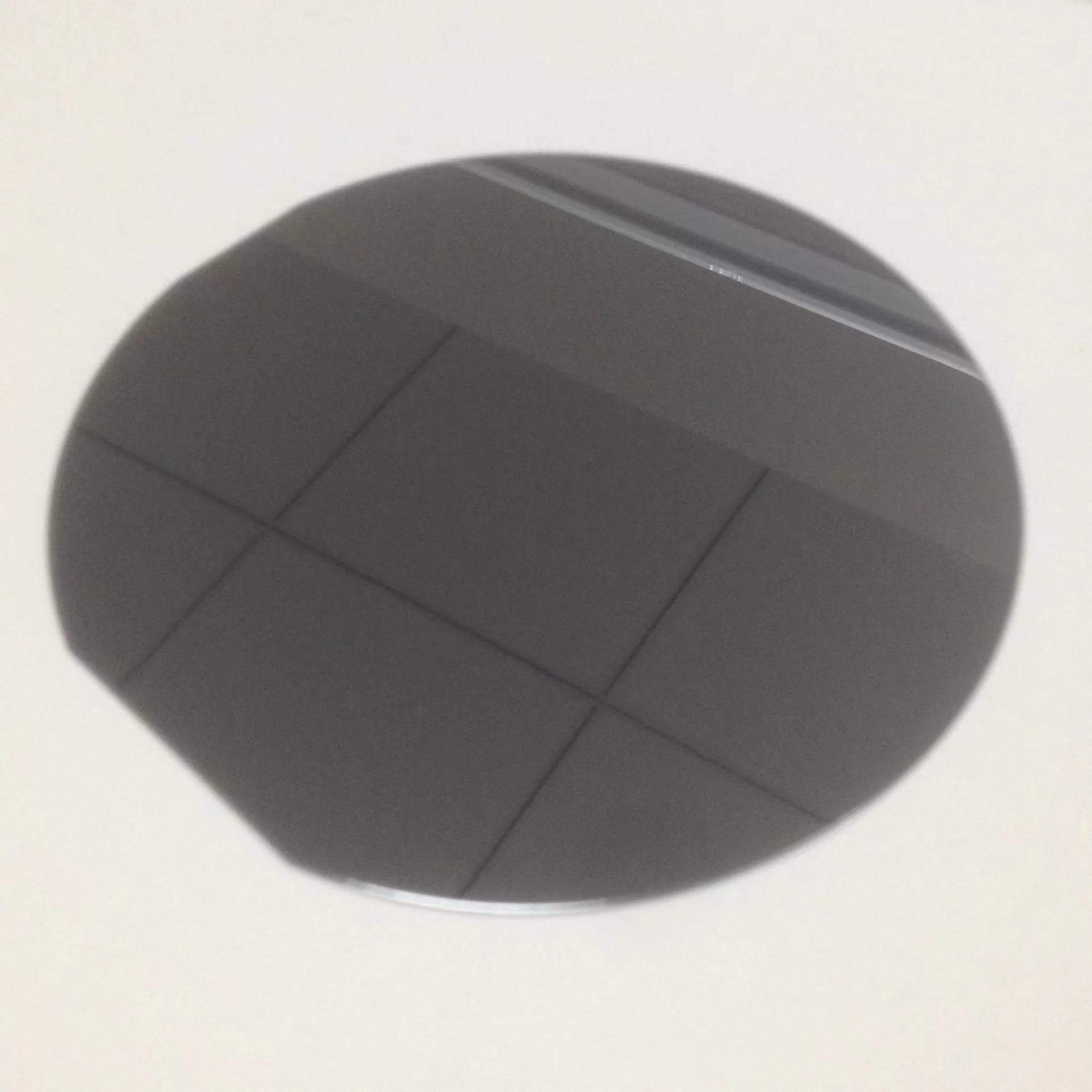
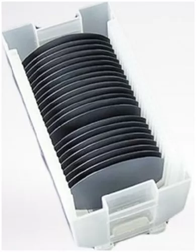
TGV Through Glass Vias Pictures


TGV Through Glass Vias‘s abstract
Glass is increasingly being recognized as a versatile material for advanced packaging technologies due to its inherent properties. As a superior insulator, glass exhibits minimal electrical losses, especially at higher frequencies. Its high stiffness and tunable thermal expansion coefficient help in managing warp in glass core substrates and bonded stacks, which is crucial for applications involving through glass vias (TGV) and carrier systems. Moreover, glass offers cost-effective advantages; its forming processes can produce components in panel formats and in thicknesses as thin as 100 micrometers. This capability allows for the potential refinement or even elimination of traditional manufacturing techniques.
With the growing adoption of glass in the industry, significant progress has been made in enhancing downstream processes, including glass handling and via/surface metallization. An interesting development is the utilization of existing tool sets and processes originally designed for panel fabrication, which helps achieve the cost efficiencies demanded by the industry. In this update, we discuss the latest advancements in these processes and handling techniques that support efficient manufacturing workflows. Additionally, we highlight recent demonstrations that underscore the electrical, thermal, and mechanical reliability of glass in advanced packaging applications.
TGV Through Glass Vias‘s product application
Through Glass Vias (TGV) technology has a broad range of applications across various industries due to its ability to provide reliable, high-density electrical interconnections through glass substrates. Here are some of the key product applications of TGV Through Glass Vias technology:
- Consumer Electronics: TGVs are widely used in the manufacturing of smartphones, tablets, and other portable devices. They help in reducing the size and weight of these devices while enhancing performance by improving the integration of multiple functions onto a single chip.
- Optoelectronics and Photonics: TGV Through Glass Vias technology is critical in the production of optoelectronic devices such as LEDs, laser diodes, and photodetectors. In photonics, TGVs are used for creating glass interposers that can house optical components, allowing for efficient light transmission and reducing signal loss.
- Radio Frequency (RF) Modules: TGV Through Glass Vias provide excellent electrical insulation and low electrical loss at high frequencies, which is beneficial for RF applications. They are used in RF modules for wireless communication devices to enhance signal integrity and reduce interference.
- Medical Devices: The biocompatibility and hermetic sealing capabilities of glass make TGVs suitable for medical implants and diagnostic equipment. They can be used to create compact, reliable packages that protect sensitive electronics in medical environments.
- Automotive Electronics: In automotive applications, TGV Through Glass Vias contribute to the development of more reliable and robust electronic systems, such as sensors and control units that must perform under harsh environmental conditions.
- High-Performance Computing: TGV Through Glass Vias technology is used in high-performance computing for creating high-density interconnects in multi-chip modules and advanced processors. This helps in improving data transfer speeds and reducing latency.
- Aerospace and Defense: The reliability and durability of TGVs under extreme conditions make them suitable for aerospace and defense applications, where they are used in avionics, satellite communications, and other critical electronic systems.
- MEMS Devices: Micro-Electro-Mechanical Systems (MEMS) benefit from TGV Through Glass Vias technology for integrating electronic and mechanical components in a single glass substrate, leading to miniaturization and enhanced performance of devices like accelerometers and gyroscopes.
The versatility and superior properties of TGVs, such as low electrical loss, high stiffness, and customizable thermal expansion, continue to expand their applications in various high-tech fields, driving innovations in electronic packaging and device integration.
TGV Through Glass Vias‘s product feature
Through Glass Vias (TGV) technology offers several distinct product features that make it highly valuable for advanced electronic packaging and interconnection solutions. Here’s a breakdown of these features and how they contribute to the effectiveness of TGV technology:
- Electrical Insulation: Glass is an excellent electrical insulator, which helps in minimizing electrical losses and interference. This feature is particularly beneficial at high frequencies, making TGVs ideal for RF applications and high-speed data transmission.
- Low Dielectric Constant: The low dielectric constant of glass reduces capacitive coupling between conductive paths through the substrate. This is crucial for maintaining signal integrity in high-speed applications, such as in telecommunications and data centers.
- High Mechanical Strength: Glass substrates are known for their high stiffness and mechanical strength, which provides robustness to the overall package. This is particularly important in applications that require high reliability under mechanical stress or vibration, such as automotive and aerospace electronics.
- Thermal Stability: Glass has a stable coefficient of thermal expansion (CTE), which can be tailored to match those of other materials used in semiconductor packaging. This reduces thermal stress and improves the reliability of the bonded interfaces in fluctuating temperatures.
- Chemical Resistance: Glass is chemically inert and resistant to many environmental factors, including moisture and corrosive chemicals. This makes TGVs suitable for use in harsh environments and extends the lifespan of electronic components.
- Hermetic Sealing: TGV Through Glass Vias technology can be used to create hermetically sealed packages that protect sensitive electronics from environmental contaminants. This is especially valuable in medical and military applications where device integrity and longevity are critical.
- Scalability and Flexibility in Design: TGV Through Glass Vias processes allow for flexibility in designing vias with various diameters and at different densities. This adaptability makes it possible to optimize designs for specific applications, whether it’s for high-density interconnects in consumer electronics or for robust interconnects in industrial applications.
- Cost-Effectiveness: Despite the advanced capabilities, TGV technology can be cost-effective. The use of glass, coupled with scalable manufacturing processes, allows for economical production especially in panel formats which suit large-scale manufacturing.
- Compatibility with Existing Manufacturing Processes: TGV Through Glass Vias technology integrates well with standard semiconductor processes, including lithography and metallization. This compatibility facilitates easier adoption into existing production lines, reducing the need for specialized equipment.
These features make TGV technology a preferred choice for various high-tech applications, enabling the development of compact, high-performance, and reliable electronic devices.
Introduction to TGV Technology
Recent advancements in semiconductor packaging have spurred the demand for innovative material solutions. Efforts have significantly intensified to enhance interposer technology, crucial for 3D integrated circuit (IC) stacking. A variety of approaches, including traditional interposers made from commonly utilized materials and Fan-Out Wafer Level Packaging (FOWLP), are being explored to meet these demands. The latter, in particular, has gained traction as a cost-effective option.
Additionally, the surge in mobile devices and Internet of Things (IoT) technology has imposed stringent requirements on RF communications. Challenges such as accommodating multiple frequency bands, reducing package sizes, and improving power efficiency to extend battery life are becoming more critical as new features are introduced.
In response to these challenges, glass has emerged as a highly effective material. It offers several advantageous properties, such as high resistivity, minimal electrical loss, a low or tunable dielectric constant, and an adjustable coefficient of thermal expansion (CTE). Recent research has capitalized on these attributes to meet the stringent demands of modern electronic packaging.
For many RF and interposer applications, precise through-glass vias (TGVs) are essential for electrical interconnectivity and other functionalities. The techniques for drilling precise holes in glass and subsequent metallization for via creation are evolving toward mass production readiness. Recent developments have also confirmed the durability of these glass structures, particularly after rigorous thermal cycling tests.
At Corning Incorporated, significant progress has been made in perfecting high-quality vias in glass substrates across different formats. Recent demonstrations include the effective use of both through and blind vias in wafer and panel formats, which maintain the integrity and strength of the original glass. Filled vias have demonstrated excellent mechanical and electrical reliability, underscoring their robustness and effectiveness.
Current best practices for the TGV Through Glass Vias process are outlined in the accompanying table. While these practices provide a baseline, ongoing innovations continue to expand the capabilities of this technology.

In addition to providing superior technical performance, it is crucial for packaging solutions to be economically viable. Corning’s fusion forming process exemplifies a technique that enables the production of high-quality glass substrates on a large scale, significantly larger than 1 meter. This process has the capability to produce ultra-thin, flexible glass with thicknesses as minimal as approximately 100 micrometers.
By offering these large substrates in either wafer or panel formats at such reduced thicknesses, there are substantial possibilities for decreasing manufacturing expenses. The benefits of utilizing Corning’s fusion forming process to provide substrates tailored for electronics applications have been well-documented in the past.

Advantages of our materials
For sapphire materials
Sapphire material has several advantages in Through Glass Vias (TGV) applications:
- Excellent Mechanical Properties:
- Hardness and Strength: Sapphire has extremely high hardness and strength, making it more resistant to wear and scratches compared to ordinary glass. This enhances its durability during manufacturing and operation.Thermal Expansion Coefficient: Sapphire has a low thermal expansion coefficient, meaning it undergoes minimal dimensional changes with temperature fluctuations, aiding in maintaining structural stability and precision.
Superior Electrical Properties:
- Electrical Insulation: Sapphire is an excellent electrical insulator, effectively preventing current leakage. This is particularly important for microelectronic devices and high-frequency applications requiring high electrical insulation.Low Dielectric Constant and Loss: Sapphire possesses a low dielectric constant and low dielectric loss, beneficial for high-frequency and high-speed electronic applications as it reduces signal loss and delay.
Optical Properties:
- High Transparency: Sapphire is highly transparent in the visible and infrared spectrum, making it suitable for optical devices and optoelectronic applications.Optical Stability: Sapphire maintains stable optical properties under high temperatures and harsh environments, ensuring reliability in extreme conditions.
Thermal Properties:
- High Thermal Conductivity: Sapphire has high thermal conductivity, facilitating effective heat dissipation during device operation, ensuring proper functioning under high power and temperature conditions.Thermal Stability: Sapphire exhibits excellent thermal stability at high temperatures, preventing significant performance changes due to temperature fluctuations.
Chemical Stability:
- Corrosion Resistance: Sapphire is highly resistant to most chemicals, including acids and bases, prolonging the device’s lifespan.Environmental Resistance: Sapphire remains stable in harsh environmental conditions (e.g., high humidity, high radiation), preventing degradation.
Processing Precision:
- Microfabrication Capability: With advanced processing technologies (such as laser drilling and chemical mechanical polishing), sapphire can be precisely fabricated into high-quality TGVs, meeting the micro-level precision requirements of microelectronic devices.
In summary, sapphire offers numerous advantages for TGV applications, including mechanical strength, electrical insulation, thermal conductivity, chemical stability, and optical properties, making it ideal for high-performance microelectronic and optoelectronic fields. These characteristics make sapphire an ideal material for manufacturing high-quality TGVs.
For JGS1 JGS2 materials
JGS1 and JGS2 materials offer the following advantages in Through Glass Vias (TGV) technology:
- High Purity and Low Impurity Content:
- JGS1 and JGS2 are high-purity quartz glass materials with very low impurity levels, ensuring excellent electrical properties and low losses.
- Excellent Optical Performance:
- These materials exhibit high transmittance and low absorption, especially in the ultraviolet to infrared spectrum, which is beneficial for optical communication and sensing applications.
- Low Thermal Expansion Coefficient:
- JGS1 and JGS2 have extremely low thermal expansion coefficients, enabling them to maintain dimensional stability under temperature variations and reducing thermal stress on TGV Through Glass Vias structures.
- High Mechanical Strength and Hardness:
- They possess high mechanical strength and hardness, capable of withstanding the mechanical stresses during TGV Through Glass Vias fabrication and subsequent usage.
- Chemical Stability and Corrosion Resistance:
- Quartz glass demonstrates excellent resistance to most chemicals, ensuring stability in chemical environments and prolonging the lifespan of TGV Through Glass Vias components.
- High Thermal Conductivity:
- These materials have relatively high thermal conductivity, aiding in heat dissipation and preventing electronic devices from overheating.
- Excellent Electrical Insulation Properties:
- JGS1 and JGS2 exhibit high electrical resistivity as insulation materials, suitable for high-frequency and high-voltage applications to minimize leakage and short-circuit risks.
- Good Machinability:
- Due to their material properties, JGS1 and JGS2 are easily machinable, polished, and cleaned, allowing for the production of high-precisionTGV Through Glass Vias structures.
These advantages make JGS1 and JGS2 ideal materials for TGV Through Glass Vias technology, meeting the demands of high-performance and high-reliability applications.
For quartz materials
Quartz materials offer several advantages in Through Glass Vias (TGV) technology:
- High Purity and Low Impurity Content:
- Quartz materials are of high purity with very low impurity levels, ensuring excellent electrical properties and minimal signal loss.
- Excellent Optical Performance:
- Quartz exhibits high transmittance and low absorption in a wide range of wavelengths from ultraviolet to infrared, making it suitable for optical communication and sensing applications.
- Low Thermal Expansion Coefficient:
- Quartz has an extremely low thermal expansion coefficient, maintaining dimensional stability under varying temperatures and reducing thermal stress on TGV structures.
- High Mechanical Strength and Hardness:
- Quartz materials possess high mechanical strength and hardness, enabling them to withstand the mechanical stresses encountered during TGV Through Glass Vias fabrication and subsequent usage.
- Chemical Stability and Corrosion Resistance:
- Quartz is highly resistant to most chemicals, ensuring stability in various chemical environments and prolonging the lifespan of TGV Through Glass Vias components.
- High Thermal Conductivity:
- Quartz materials have relatively high thermal conductivity, aiding in effective heat dissipation and preventing electronic devices from overheating.
- Excellent Electrical Insulation Properties:
- Quartz exhibits high electrical resistivity, making it an excellent insulator for high-frequency and high-voltage applications, thereby minimizing leakage and short-circuit risks.
- Good Machinability:
- Quartz materials are easily machinable, polishable, and cleanable, allowing for the production of high-precision TGV structures.
These advantages make quartz materials ideal for TGV technology, meeting the demands of high-performance and high-reliability applications.
Q&A
What is through glass via TGV technology?
Through Glass Via (TGV) technology is an advanced fabrication technique used primarily in the electronics industry for creating high-density interconnections in electronic packages. TGVs are vertical electrical interconnects that pass through glass substrates, offering several benefits over traditional interconnect methods. Here is a detailed explanation of TGV technology:
Overview of TGV Technology
1. Definition and Purpose:
- TGV technology involves drilling or etching small holes (vias) through glass wafers and subsequently filling these holes with conductive materials, such as copper or other metals, to create vertical electrical connections. This allows for the interconnection of different electronic components or layers within a package.
2. Key Components:
- Glass Substrate: The base material is typically a high-purity, low-impurity glass, such as quartz or borosilicate glass, chosen for its excellent electrical and thermal properties.
- Via Formation: Vias are created using precise laser drilling, deep reactive ion etching (DRIE), or other microfabrication techniques.
- Metallization: The vias are then metallized, usually with copper or other conductive materials, to form the electrical pathways.
Advantages of TGV Technology
1. Electrical Performance:
- Low Signal Loss: Glass has excellent dielectric properties, leading to minimal signal loss and better performance at high frequencies.
- High Insulation: Glass substrates provide superior electrical insulation, reducing crosstalk and electromagnetic interference.
2. Thermal Management:
- Low Thermal Expansion: Glass materials have a low thermal expansion coefficient, reducing thermal stress and ensuring stability in temperature variations.
- Efficient Heat Dissipation: TGV structures can be designed to enhance heat dissipation, improving the reliability and performance of electronic devices.
3. Mechanical Properties:
- High Strength and Stability: Glass substrates offer high mechanical strength and dimensional stability, which is crucial for maintaining the integrity of fine-pitch interconnects.
- Chemical Resistance: Glass is chemically inert and resistant to corrosion, enhancing the durability of the electronic package.
4. Miniaturization and Integration:
- High-Density Integration: TGV technology allows for the creation of very fine-pitch interconnects, enabling higher density packaging and the integration of more components in a smaller footprint.
- Three-Dimensional Integration: TGVs facilitate 3D integration of electronic components, leading to more compact and efficient designs.
Applications of TGV Technology
1. Advanced Packaging:
- TGVs are used in advanced packaging solutions, such as System-in-Package (SiP) and heterogeneous integration, where multiple semiconductor devices and passive components are integrated into a single package.
2. MEMS and Sensors:
- Micro-Electro-Mechanical Systems (MEMS) and various sensors benefit from TGV technology due to the need for high-density interconnections and the excellent mechanical and thermal properties of glass.
3. Optoelectronics:
- TGVs are crucial in optoelectronic applications, including photonic devices and integrated optical circuits, where low-loss optical transmission and high precision are required.
4. High-Frequency Applications:
- Due to the superior electrical properties of glass, TGVs are ideal for high-frequency RF and microwave applications, including communication devices and radar systems.
Fabrication Process of TGVs
1. Via Formation:
- Laser Drilling: A laser is used to precisely drill holes through the glass substrate. This method offers high precision and can create vias with very small diameters.
- Reactive Ion Etching (RIE): An alternative to laser drilling, RIE uses plasma to etch vias through the glass with high aspect ratios and smooth sidewalls.
2. Metallization:
- Seed Layer Deposition: A thin conductive seed layer, often copper, is deposited inside the vias and on the surface of the glass.
- Electroplating: The vias are then filled with copper or another conductive material through electroplating, ensuring a solid and continuous electrical path.
- Planarization: The surface of the glass is planarized to remove excess metal and ensure a smooth and even surface.
3. Assembly and Integration:
- Bonding: The glass substrate with TGVs is bonded to other components or substrates using various bonding techniques such as direct bonding, anodic bonding, or adhesive bonding.
- Packaging: The final assembly is packaged and encapsulated to protect the delicate interconnects and ensure the reliability of the device.
Conclusion
TGV technology represents a significant advancement in electronic packaging, offering numerous advantages in terms of electrical performance, thermal management, mechanical stability, and integration density. Its applications span a wide range of fields, including advanced semiconductor packaging, MEMS, sensors, optoelectronics, and high-frequency devices. The precise fabrication process, involving sophisticated techniques for via formation and metallization, ensures the high performance and reliability of TGV-based interconnects, making it a crucial technology in the development of next-generation electronic devices.
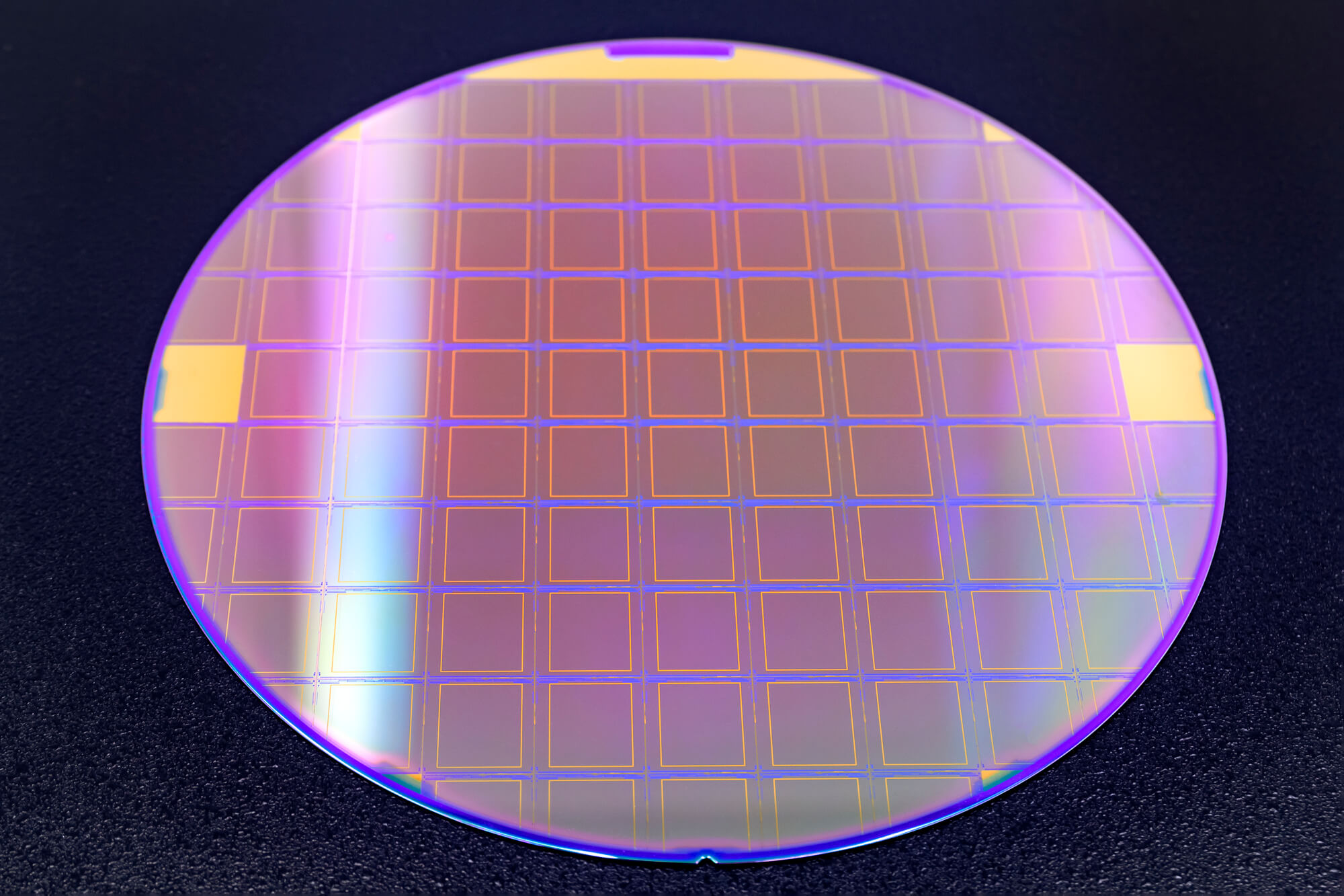


 on Silicon (Si) Epitaxy Wafer 3")
