
8inch SiC wafer’s abstract
8-inch SiC wafers are increasingly gaining popularity and demand in various industries. As the market for SiC wafers expands, there is a growing need for these high-quality substrates to support research, development, and commercial applications. With their exceptional properties and wide-ranging potential, 8-inch SiC wafers are becoming the preferred choice for semiconductor manufacturers, researchers, and innovators worldwide. Their versatility, reliability, and performance make them indispensable in the advancement of next-generation electronics, power devices, and renewable energy technologies. The growing recognition of the benefits offered by 8-inch SiC wafers underscores their significance in driving innovation and shaping the future of various industries.
8-inch SiC wafer substrates with silicon carbide, available in thicknesses of 500μm and 350μm. These wafers are of the 4H-N type, suitable for prime, dummy, and research-grade applications. Our product summary includes:
High-quality SiC wafers designed for research and experimentation purposes.
Ability to provide small quantities, special specifications products, and customized services to meet diverse needs.
Global shipping services with secure payment options and a large inventory to ensure availability.
Minimum delivery time within 1 week, shipped by reliable carriers such as FedEx, DHL, UPS, etc.
Feel free to reach out for further details or to place an order.
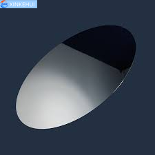
8inch SiC wafer’s photo
8inch SiC wafer
8inch-sic-wafer
8inch SiC wafer’s properties
The properties of 8-inch SiC (silicon carbide) wafers make them highly desirable for a wide range of applications in various industries. Some key properties include:
Wide Bandgap: 8inch SiC wafers possess a wide bandgap, typically around 3.2 to 3.4 eV for 4H-SiC, enabling them to operate at higher temperatures and voltages compared to silicon wafers. This property is crucial for power electronics, where high-temperature and high-voltage operation is required.
High Thermal Conductivity: 8inch SiC wafers exhibit excellent thermal conductivity, allowing for efficient heat dissipation. This property is essential for power devices and high-power electronic circuits, as it helps in managing heat generation and improving device reliability.
High Breakdown Electric Field Strength:8inch SiC wafers have a high breakdown electric field strength, which enables them to withstand high voltages without breakdown. This property is advantageous for power devices, where high voltage operation is necessary.
High Electron Mobility: 8inch SiC wafers have high electron mobility, which contributes to their excellent performance in high-frequency and high-power electronic applications. This property is beneficial for RF (radio frequency) devices, microwave devices, and high-speed power switching applications.
Chemical and Mechanical Stability: 8inch SiC wafers exhibit excellent chemical and mechanical stability, making them resistant to harsh environments, corrosion, and mechanical stress. This property enhances their reliability and durability in various applications.
Low Power Losses: 8inch SiC wafers have lower power losses compared to silicon wafers, particularly at high frequencies and temperatures. This property is advantageous for power electronics, where minimizing energy losses is critical for efficiency.
Compatibility with GaN: 8inch SiC wafers are often used as substrates for gallium nitride (GaN) epitaxy, as they provide a suitable lattice match and thermal expansion coefficient. This property enables the integration of GaN-based devices with SiC-based devices, offering enhanced performance and functionality.
Property 4H-SiC Single Crystal
Lattice Parameters (Å) a=3.076c=10.053
Stacking Sequence ABCB
Density 3.21
Mohs Hardness ~9.2
Thermal Expansion Coefficient (CTE) (/K) 4-5 x 10⁻⁶
Refraction Index @750nm no = 2.61ne = 2.66
Dielectric Constant c ~ 9.66
Doping Type N-type or Semi-insulating
Thermal Conductivity (W/cm-K @298K)(N-type, 0.02 ohm-cm) a~4.2c~3.7
Thermal Conductivity (W/cm-K @298K)(Semi-insulating type) a~4.9c~3.9
Band-gap (eV) 3.23
Break-Down Electrical Field (V/cm) 3-5 x 10⁶
Saturation Drift Velocity (m/s) 2.0 x 10⁵
Wafer and Substrate Sizes Wafers: 2, 4, 6, 8 inch; smaller substrates: 10×10, 20×20 mm, other sizes are available and can be custom-made upon request
8inch SiC wafer’s applications
8-inch SiC (silicon carbide) wafers find applications across various industries due to their unique properties and performance advantages. Some of the key applications include:
Power Electronics: 8inch SiC wafers are extensively used in power electronic devices such as Schottky diodes, MOSFETs (Metal-Oxide-Semiconductor Field-Effect Transistors), JFETs (Junction Field-Effect Transistors), and IGBTs (Insulated Gate Bipolar Transistors). They offer higher breakdown voltage, lower on-state resistance, and faster switching speeds compared to traditional silicon-based devices. This makes them ideal for high-voltage and high-power applications including electric vehicles, renewable energy systems (such as solar and wind inverters), industrial motor drives, and power supplies.
RF/Microwave Devices: 8inch SiC wafers are used in the fabrication of RF (Radio Frequency) and microwave devices such as RF power amplifiers, high-frequency switches, and RF filters. Their high electron mobility and thermal conductivity enable the development of high-performance devices for communication systems, radar systems, wireless infrastructure, and satellite communications.
Optoelectronics: 8inch SiC wafers are employed in optoelectronic devices such as UV (Ultraviolet) photodetectors, LEDs (Light-Emitting Diodes), and SiC-based photovoltaic cells. Their wide bandgap and high thermal conductivity make them suitable for applications requiring high-temperature and high-power operation, such as UV detection, solid-state lighting, and solar energy conversion.
High-Temperature and Harsh Environment Sensors:8inch SiC wafers are utilized in the fabrication of sensors for high-temperature and harsh environment monitoring applications. These sensors can withstand extreme temperatures, corrosive environments, and high levels of radiation, making them suitable for aerospace, automotive, industrial, and defense applications.
Semiconductor Research and Development:8inch SiC wafers serve as essential substrates for semiconductor research and development, enabling the fabrication and characterization of novel electronic devices and materials. Researchers use SiC wafers to explore new device architectures, study material properties, and advance the field of wide-bandgap semiconductors.
Overall, the versatility, reliability, and superior performance of 8-inch SiC wafers make them indispensable in various cutting-edge technologies, driving innovation and advancements across multiple industries.
8inch SiC wafer’s advantages
In light of current geopolitical tensions, the advantages of 8-inch SiC wafers become even more pronounced, offering strategic benefits in several key areas:
Diversification of Supply Chains: With disruptions and uncertainties affecting global supply chains, the production of 8-inch SiC wafers offers an opportunity for diversification. Manufacturers can reduce reliance on specific regions or countries for semiconductor materials, thereby mitigating geopolitical risks and ensuring continuity of supply.
Enhanced National Security: As governments around the world prioritize national security concerns, the domestic production of 8-inch SiC wafers strengthens semiconductor self-sufficiency. By reducing dependence on foreign suppliers, countries can safeguard critical technologies and infrastructure from potential disruptions or hostile actions.
Technological Innovation: The production of 8-inch SiC wafers fosters technological innovation and R&D capabilities within domestic semiconductor industries. Investing in advanced materials like silicon carbide enables the development of next-generation semiconductor devices with superior performance, efficiency, and reliability, driving progress in key sectors such as power electronics, telecommunications, and defense.
Competitive Advantage: Countries or companies with the capability to produce high-quality 8-inch SiC wafers gain a competitive edge in the global semiconductor market. By offering reliable and cutting-edge materials, they attract customers seeking advanced solutions for their applications, thus strengthening their position in the industry and expanding market share.
Resilience to Trade Restrictions: In an environment of escalating trade tensions and export controls, domestic production of 8-inch SiC wafers provides resilience against trade restrictions imposed by foreign governments. By fostering a self-sufficient supply chain, countries can mitigate the impact of export bans or tariffs on critical semiconductor materials, ensuring the continuity of key industries and technologies.
In summary, the advantages of 8-inch SiC wafers extend beyond technological capabilities, encompassing strategic considerations related to supply chain resilience, national security, technological innovation, and competitive positioning amidst evolving geopolitical dynamics. By investing in the production of these advanced semiconductor materials, countries and companies can fortify their positions in the global semiconductor landscape and navigate geopolitical challenges more effectively.
6 Inch N Type Polished Silicon Wafer in hot demand Prime silicon wafer for semiconductor Solar Cells P type N type,2 to 12inch SIO2 Silicon Dioxide Wafer Thickness 10um-25um 6 Inch 8 Inch Gallium Phosphide GaP wafers Bandgap Light-Emitting Diodes 4H N-TYPE SIC SUBSTRATE Ideal High-Temperature Stable Materials


 on Silicon (Si) Epitaxy Wafer 1")