Applications
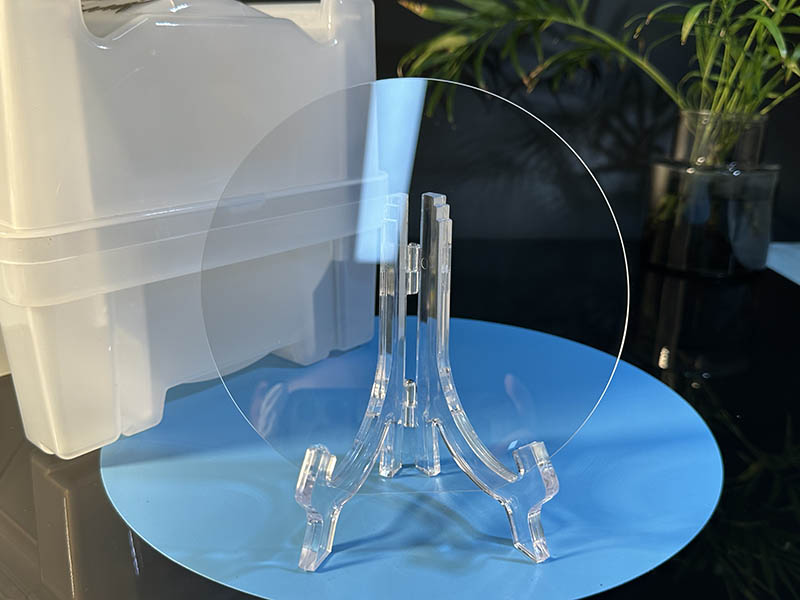
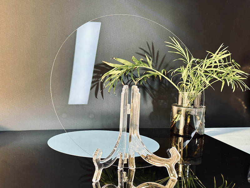
Applications for 6-inch sapphire wafers include:
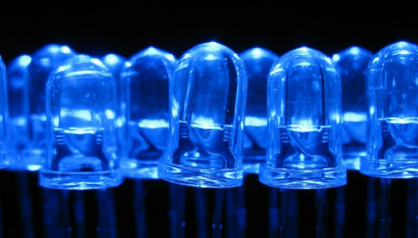
1. LED manufacturing: sapphire wafer can be used as the substrate of LED chips, and its hardness and thermal conductivity can improve the stability and service life of LED chips.
2. Laser manufacturing: Sapphire wafer can also be used as the substrate of laser, to help improve the performance of laser and prolong the service life.
3. Semiconductor manufacturing: Sapphire wafers are widely used in the manufacture of electronic and optoelectronic devices, including optical synthesis, solar cells, high-frequency electronic devices, etc.
4. Other applications: Sapphire wafer can also be used to manufacture touch screen, optical devices, thin film solar cells and other high-tech products.
Specification
| Material | High purity single crystal Al2O3, sapphire wafer. |
| Dimension | 150 mm +/- 0.05 mm, 6 inch |
| Thickness | 1300 +/- 25 um |
| Orientation | C plane (0001) off M (1-100) plane 0.2 +/- 0.05 degree |
| Primary flat orientation | A plane +/- 1 degree |
| Primary flat length | 47.5 mm +/- 1 mm |
| Total Thickness Variation (TTV) | <20 um |
| Bow | <25 um |
| Warp | <25 um |
| Thermal Expansion Coefficient | 6.66 x 10⁻⁶ / °C parallel to C axis, 5 x 10⁻⁶ /°C perpendicular to C axis |
| Dielectric Strength | 4.8 x 10⁵ V/cm |
| Dielectric Constant | 11.5 (1 MHz) along C axis, 9.3 (1 MHz) perpendicular to C axis |
| Dielectric Loss Tangent (a.k.a. dissipation factor) | less than 1 x 10⁻⁴ |
| Thermal Conductivity | 40 W/(m.K) at 20℃ |
| Polishing | single side polished (SSP) or double side polished (DSP) Ra < 0.5 nm (by AFM). The reverse side of SSP wafer was fine ground to Ra = 0.8 – 1.2 um. |
| Transmittance | 88% +/-1 % @460 nm |
Detailed Diagram


